
What is the cost of PCB Manufacture & Assembly for The Heart?
Prices Start From $1000
Our PCB Manufacturing and PCB Assembly (PCBA) services offer small to large volume production. We also provide electronic design and prototyping services, if needed. Alternatively, just send us your gerber files, BOM, centroid (XY) data, board specs and quantity. Our engineers will work closely with you, to aim for the best quality and quickest possible lead time.
Cost-effective PCBA: low overheads, passing savings onto our customers.
Rapid PCBA: quotes back in about 48 hours.
Informative production: daily or weekly progress updates.
PCBA made easy - gotta love the power of stencils, reflow ovens, and pick & place robots.
We also offer Electronic Design, PCB Rework, and Software Development services for The Heart, as part of our New Product Development suite of services.

PCB Capabilities
| Items | Manufacturing Capabilities | Remarks |
|---|---|---|
| Number of Layers | 1-10 layers | For orders above 10 layers, please contact us. |
| Material | FR-4, Aluminum | For Flex, Rigid-flex, Metal-based (Aluminum etc.), HDI, Halogen-free, High Tg, etc. - please contact us. |
| Maximum PCB Size (Dimension) | 500x1100 mm | Any sizes beyond this dimension - please contact us. |
| Board Size Tolerance (Outline) | ±0.2mm / ±0.5mm | ±0.2mm for CNC routing, and ±0.5mm for V-scoring. |
| Board Thickness | 0.4-2.4mm | 0.4, 0.6, 0.8, 1.0, 1.2, 1.6, 2.0, 2.4mm. Please contact us if your board exceeds these. |
| Board Thickness Tolerance (t ≥ 1.0mm) | ±10% | Normally "+ Tolerance" will occur due to PCB processing steps such as electroless copper, solder mask and other types of finish on the surface. |
| Board Thickness Tolerance (t < 1.0mm) | ±0.1mm | Normally "+ Tolerance" will occur due to PCB processing steps such as electroless copper, solder mask and other types of finish on the surface. |
| Min Trace | 0.1mm / 4mil | Min manufacturable trace is 4mil (0.1mm), strongly suggest to design trace above 6mil (0.15mm) to save cost. |
| Min Spacing | 0.1mm / 4mil | Min manufacturable spacing is 4mil (0.1mm), strongly suggest to design spacing above 6mil (0.15mm) to save cost. |
| Outer Layer Copper Thickness | 1oz / 2oz / 3oz (35μm / 70μm / 105μm) | Also known as copper weight. 35μm = 1oz, 70μm = 2oz, 105μm = 3oz. Please contact us if you need copper weight greater than 3oz. |
| Inner Layer Copper Thickness | 1oz / 1.5oz (35μm / 50μm) | Inner copper weight as per customer’s request for 4 and 6 layers. Please contact us if you need copper weight greater than 1.5oz. |
| Drill Sizes (CNC) | 0.2-6.3mm | Min drill size is 0.2mm, max drill is 6.3mm. Any holes greater than 6.3mm or smaller than 0.3mm will be subject to extra charges. |
| Min Width of Annular Ring | 0.15mm (6mil) | For pads with vias in the middle, Min width for Annular Ring is 0.15mm (6mil). |
| Finished Hole Diameter (CNC) | 0.2-6.2mm | The finished hole diameter will be smaller than size of drill bits because of copper plating in the hole barrels |
| Finished Hole Size Tolerance(CNC) | ±0.08mm | For example, if the drill size is 0.6mm, the finished hole diameter ranges from 0.52mm to 0.68mm will be considered acceptable. |
| Solder Mask | LPI | Liquid Photo-Imageable is the mostly adopted. Thermosetting Ink is used in the inexpensive paper-based boards. |
| Minimum Character Width (Legend) | 0.15mm | Characters of less than 0.15mm wide will be too narrow to be identifiable. |
| Minimum Character Height (Legend) | 0.8mm | Characters of less than 0.8mm high will be too small to be recognizable. |
| Character Width to Height Ratio (Legend) | 1:5 | In PCB silkscreen legends processing, 1:5 is the most suitable ratio |
| Minimum Diameter of Plated Half Holes | 0.6mm | Design Half-Holes greater than 0.6mm to ensure better connection between boards. |
| Surface Finishing | HASL with lead, HASL lead free, Immersion gold | The most popular three types of PCB surface finish. Please contact us for other finishes. |
| Solder Mask | Green, Red, Yellow, Blue, White, Black | No extra charge (Green, Red, Yellow, Blue) |
| Silkscreen | White, Black, None | No extra charge. |
| Panelization | V-scoring, Tab-routing, Tab-routing with Perforation (Stamp Holes) | Leave min clearance of 1.6mm between boards for break-routing. For V-score panelization, set the space between boards to be zero. |
| Others | Fly Probe Testing (Free) and A.O.I. testing(free), ISO 9001:2008, UL Certificate | No extra charge. |
PCB Manufacture & Assembly for Gippsland, Victoria, Australia
At COLETEK, we empower businesses in Gippsland, Victoria, Australia, to harness the power of innovative electronics and precision manufacturing. Our comprehensive PCB Manufacture & Assembly services streamline the process from design conception to production-ready deployment.
Our experienced engineers collaborate closely with clients to capture requirements, refine designs, and navigate technical trade-offs. We seamlessly integrate components, ensuring optimal functionality and performance. Our iterative approach involves regular design reviews, testing, and refinement to ensure your vision becomes reality.
We understand the unique challenges of remote locations and prioritize seamless collaboration across regional and metropolitan clients. Our in-house prototyping lab facilitates rapid hardware and software development, testing, and refinement. This ensures efficient progress from proof-of-concept work through production-readiness planning.
COLETEK has successfully delivered over 150 R&D and new product development projects for clients across industries. Our proven track record and client-centric approach make us the trusted partner for PCB Manufacture & Assembly in Gippsland, Victoria, Australia.
Let us leverage our expertise to empower your business to innovate, iterate, and achieve remarkable outcomes. Contact COLETEK today to discuss your project and discover how we can help you bring your vision to life.
Let’s build something remarkable together.
Contact UsPCB Manufacture & Assembly for The Heart – Our Clients: Big Brands & Small Businesses


PCB Manufacture & Assembly for The Heart – Amazing Customer Testimonials
We worked with Luke from COLETEK to develop a prototype for a new venture. Luke was able to give us practical advice on how to execute the project inline with our budget that was super useful. What has been endearing, is that even after the build was complete, Luke continues to touch base with us offering help to keep the momentum of the project going forward.

We've worked with Luke and the team on and off for the past two years. We've found them very accessible and extremely thorough in their dealings. Their documentation is second to none and we’d have no hesitation recommending them on this basis alone.
COLETEK have been absolutely fantastic in their support and manufacture of various components for us. Our designs are always bespoke, intricate and low volume and it’s great to have an Australian company like COLETEK as a trusted and quality manufacturer for our spacecraft mechanical components and assemblies – which have been flight proven through successful mission operations. Keep up the great work!
I'm in the early stages of my prototype design. I have worked with Luke for a couple of years now and in that time I have found Luke to be very reliable, responsible with my design, honest and trustworthy. What stood out the most was Luke's pride and commitment that he undertakes to ensure a positive outcome. I consider it a privilege to call Luke an associate and have no hesitation in encouraging others to do the same.
Luke and the team do a amazing job. Extremly happy from start to finish
We met with Luke Cole from COLETEK and very quickly realised that he was very knowledgeable in robotics and prototyping. What separates his company from the rest, is that he had a unique value proposition - COLETEK offers a tele-operated / robotic unit for rent and with the flexibility to be modified to build proof-of-concepts. That unit lowered both the cost and time for us to produce a video showing a very challenging concept. In general COLETEK's service was great value. We would recommend them - they will get it done.

I have had the pleasure of working with Luke, our exceptional robotic product developer, over the past few years. Luke's expertise and professionalism have been pivotal in advancing our projects. Their innovative approach, attention to detail, and commitment to excellence have consistently exceeded our expectations. The quality of work and dedication Luke brings to each level of our project has significantly contributed to our success. I highly recommend COLETEK for their outstanding skills and unwavering professionalism.

Skykraft is a Canberra based company designing and developing spacecraft for the delivery of global space-based services. Luke and the team have been very responsive with quotes and delivery of machined parts for our company. Looking forward to working with COLETEK on our space programmes.

Great prototype product made to our specs with minimal fuss. Delivered on time and within budget. Thanks team.

COLETEK have provided one to one communication throughout the development process and gone above and beyond in bringing our ideas closer to becoming a reality! Luke's expertise and knowledge with computer software and electronics is Jedi like, but what I liked most about working with him was his willingness and ability to think outside of the box.

Delivered excellence on time, great work and great team, thanks!

I engaged COLETEK several years ago to produce designs and working prototypes of 2 products I am currently developing as I was having difficulty obtaining what I required from overseas design companies. I have always found Luke easy to work with and having face to face meetings made explaining my concepts so much easier than endless emails. Design changes and modifications are always produced in a timely fashion and available for pickup locally.
I would thoroughly recommend COLETEK they provided me with excellent feedback and engineering knowledge with regards to our idea. They also have continued to help us with what direction we should take and introduced us to other professionals that have also guided us. I suggest anyone who has been thinking of something they would like to pursue should contact them to get the most realistic approach of making it successful.
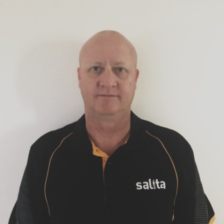
Salita engaged Luke Cole to troubleshoot issues we were having with a drive motor system with a dynamic variance of torque and speed. After approaching no less than a dozen Australian supplier and engineering firms to provide a solution, and after 12 months of product design and testing, they could not verify why their recommended motors where failing and reversing suddenly. Luke undertook testing and analysis and quickly supplied information on the failures. Not only did Luke uncover a rare, uncommon failure but also provided a solution. The COLETEK team are our go to for the correct solution the first time, for all our electronic needs.
We had the pleasure of doing business with COLETEK who provided us with service work. Their level of service and the quality of their work is exceptional. They communicated with us through the entire process to let us know when the work would be completed. We are very happy to have worked with them.

Our company has been working with COLETEK and Luke Cole for several years. Luke is very intelligent in many areas and has provided us with excellent designs and service. With the addition of a marketing section to provide brochures, packaging, etc. COLETEK is a one-stop shop. Based on our experience, we would highly recommend Luke and his company.

We engaged COLETEK to conduct a series of research projects on robotics and we very pleased with their technical skill, creative thinking and hard work. If you need to prototype a complex technical idea, they are a great partner to work with.

Thank you for your recent help with my enquiry. I have been able to proceed with my project which was proving very difficult before I was fortunate enough to make your acquaintance. The help you have given me and the contacts I have made with your support has been invaluable. Thank you so much and I look forward to a long and fruitful association.
We used COLETEK on a small project involving mechanical and electronic design aspects as well as software development. COLETEK understood our requirements at the outset and worked to accommodate our needs. The whole process was professionally conducted and we highly recommend COLETEK

From an idea in my head to making sales nationwide and now worldwide. COLETEK were there every step of the way. The product was my first development so I had no idea really. With COLETEK offering privacy agreements and steering me in the right direction, it gave me confidence instantly. One thing that may seem irrelevant they questioned me about what it was I was trying to achieve and if in fact if it's even viable? That for me showed COLETEK wasn't in it just for my money. After some meetings and a couple of CAD drawings we had our first working prototype. COLETEK's knowledge and experience definitely made this whole process a lot easier. From CAD drawings, prototypes, liaising with suppliers in Australia and overseas - COLETEK done the lot. I'd highly recommend COLETEK!
We had an idea that needed very complex design and prototype requirements. After much frustration dealing with other prototyping companies both in Australia and overseas we came across Coletek and have not looked back. Luke has been extremely helpful to date and we are now on the road to developing the product we had envisioned. Luke has been more than capable of taking multiple and constantly changing design facets in his stride and has ultimately given us a clear path to a successful product.
Intuitive, innovative & efficient are three words that would appropriately describe the COLETEK service. Luke and the team at COLETEK have taken our concepts to the next level.

COLETEK proved to be the perfect choice to help us kick our project off. Their analysis of the problem we presented with them with, and their suggestions for the most efficient and effective way to achieve a solution prevented us wasting time and money heading down the wrong path. I'd recommend COLETEK without any reservations.

I had a technical design and prototype job I needed done and had contacted two companies in Brisbane before I discovered COLETEK. From my first conversation with Luke, I knew that he was the best person for the job and he delivered under budget and within the required timeframe. The device he manufactured for my company will save us thousands of dollars and it is highly likely that we will on-sell the device to similar organisations. I recommend COLETEK for any design and prototype work you can imagine for your business.

I can say that I've only dealt once with Luke Cole at COLETEK and I found him to be very professional and helpful with his assessment of my device. His expertise and suggestions with regards to my invention was great, despite my pedestrian review of it and what I was hoping it could achieve. In the end his advice was paramount in my final decision as to whether I would move forward with the development of a prototype.

Great delivery, and great relationship orientated services.

Our dealings with COLETEK were pleasant and professional. Luke was kind and courteous and very easy to talk to. High quality design concepts were emailed through with regularity so that we always knew exactly what was going on. I would recommend supporting hard workers and local Australia business by working with COLETEK
In the development of our new product Smart Syphon we had a tight deadline to launch the commercial version of our product and experienced some issues with our drawings. Luke and his team dealt with the issues, worked through the week-end and delivered a quality outcome on time.

Luke (COLETEK) did an amazing job helping me take an idea through technical design, proof of concept and prototype development. Luke immediately understood the requirements, delivered to a budget, within the required timeframe and the whole process was extremely professional. I highly recommend for any design and prototype work you can imagine.

I consulted COLETEK for some work, commencing in 2014, and haven’t looked back. The project was very important to me, and COLETEK not only saw that but exuded sincere enthusiasm about the project; they are attentive, and thorough in their research and development service. They are a wealth of information and advice, for many aspects of the entire engineering and commercialization space, and this has been invaluable to me. I look forward to continuing work with them long into the future!

Luke has a very broad depth of knowledge across many engineering disciplines and has a large project base to draw experience from. I engaged COLETEK for assistance in some early electro-mechanical design for a hoisting system. They've been a great resource for helping develop ideas.
Over five years, we've partnered with COLETEK to deliver a sensational end-to-end product. Their expertise across hardware and software development has streamlined and expedited our project to market, achieving great success.

Luke from COLETEK has assisted us on a number of occasions and has always been helpful, courteous and understanding of our needs. There was an instance when timing was of the essence and Luke was able to prioritise our job to ensure we weren't affecting our customers in a negative way. He is highly recommended.
Founded in 2001, we are a multiple award winning, highly experienced multidisciplinary company specialising in lean product development through rapid prototyping - transforming ideas from concept to life. Our industry-leading team combines deep expertise, cutting-edge technology, and advanced equipment to validate emerging ideas—transforming them into market-ready hardware and software solutions.
Our experience dates back to the 1990s with ANU "Robotics Systems Lab", CSIRO, NICTA (aka Data61), Seeing Machines, Location Aware Technologies, and Hemisphere GPS (aka BEELINE). For over 10 years now, we've been focused on validating R&D and taking ideas to commercialisation.
Useful Links
Location
Servicing worldwide, notably:
Australia, NZ, UK, USA, Canada, Europe, UAE, and Asia